Showing posts with label DipTrace. Show all posts

Thursday, August 13, 2015

DipTrace 2.9 Beta

DipTrace has just made available Update 2.9 Beta, which includes several new capabilities or functions. The most interesting/useful to me is "Configurable HotKeys".

I have assigned:
  •       "]" to Object -> "Update All Copper Pours"
  • "Ctl-]" to Object -> "Unpour All Copper Pours"

During the last stages of a PCB edit, my productivity will now jump 1000%.

Previously making small trace-edits to (ensure connections or adjust) of the pours was an extremely tedious task.

Also, I have assigned:
  • "[" to View -> "Mirror"
Now a quick tap of "B" then "[", shows the the bottom side in "normal" flip-the-board-over view, which is very useful when adding Text Silkscreen to the bottom side.

And then, "T" and "[" reverts back to the normal top side view.

Note: A little Silkscreen text on each side helps orient yourself for each side.

And Yes I know "Mirror" has always been there, but it was always a "Pain-in-the-butt" to find it in the drop down menus, and therefore I seldom used it.


Thanks, DipTrace Team !!!


-- Home Page: https://WA0UWH.blogspot.com

Tuesday, August 4, 2015

Another ESP Adaptor

UPDATE: Here is some important info, watch this thread for progress:

Yes, this is yet another Esp8266 Adaptor, but this one will support an Esp-12E with its extra six pins. The side pins match the Castellated pins on the Esp-12E. Note: this Diptrace 3D rendering does not know how to correctly represent Castellated connectors.

Top Side - Esp8266 Esp-12E Adaptor
I just sent the design into OshPark.com for manufacture, the boards should be returned in about 2 weeks. The cost is $1.50 each. If all goes well, I will share the design as a Project on OshPark.

Bottom Side - Esp8266 Esp-12E Adaptor
"If", I did everything right (with no mistakes),  this should fit a 22 pin DIP socket, or a normal Protoboard with lots of available holes for jumper wires. The underside used two single row SMT 0.1 inch Headers which are available on Ebay, for example: here.

While designing this adaptor, I considered adding a few Pullup Resistors, Program and Reset switches. But, for the boards size that would require a four layer board, and would decreases Pin flexibility.

I think this adaptor will be my favourite, for small Esp8266 Protoboard development projects. The Esp-12E provides lots of I/O and is still very small (I like that).

Note: this design is the result of experimenting with a "Back-to-Back Configuration" as suggested in a previous post.


Update:


-- Home Page: https://WA0UWH.blogspot.com

Wednesday, July 9, 2014

Minima - User Interface Module

Updated with 3D Model Link, see below.

Thus far, I have been working on the Minima Alternate Tuning Method with push button switches that were hay-wired on a Protoboard.  Reliability of the switches and connecting wires were always suspect.

To solve this problem I have created a Modular User Interface (UI) that will be used with the rest of my Minima Modules. The UI will plug directly onto the Processor Board.

Here it is as designed in DipTrace,  and presented in 3D:

The UI in DipTrace 3D
And, as plugged onto the Processor Board:

As Installed
 (sorry for the poor photo quality, it was taken late last night)

The UI board was produced via the Toner Transfer Method, it is double sided and contains 23 40mil via's.

Wardy at http://wardyprojects.blogspot.com/ has rekindled my interest in building 3D component models for DipTrace.

DipTrace provides over 3500 component in their 3D Library, but rarely are the components that I use found (like simple headers, POTS, and buttons).

DipTrace uses the newer VRML2 format (and a few others) for their 3D components.

In the past I have used AC3D from http://www.inivis.com/ for my 3D needs , but I had let my License laps on an old forgotten dead workstation.

Wardy inspired me to re-purchase the AC3D software and start playing in 3D again (I hope that was a good idea!). The POT and push button switches seen in the design image above were recently created. The following is the most recent 3D part that I have created, it is a SMA PCB Edge Connector. It will be seen on future projects.

A 3D SMA PCB Edge Connector
To use AC3D, I save the component in the native format (*.ac) and then export the same part in VRML2 format, and which is saved in the same directory. Because AC3D does not read (import) VRML2 format, I have to re-export the parts if changes are made to the original.

Although AC3D does read (import ) the older VRML1 format, it does NOT read the VRML2 format (only export), the 3500 3D parts supplied by DipTrace can not be used as a template or starting point for my parts (what a waste).

I need to find a VRML2 to VRML1 converter, so far, googling has not helped.

My 3D Model Library

To promote the use of 3D Models in Published Documents I will share all of my 3D Models, the following Dropbox link is my "working and storage" space for my Electronic Parts.


Feel free to use my 3D Models as you like, but if they are used in your Published Documentation, please give me credit.

--

Wednesday, April 30, 2014

An Open Letter to DipTrace

A DipTrace Enhancement Request

Background

For many years I have been using DipTrace for Schematic Capture and PCB Layout. I have found DipTrace to be one of the most functional, easiest to use, and inexpensive software packages for both the hobbyist and professional.

Recent DipTrace Updates

In the past I had complained about DipTrace's use and access method of the schematic and layout libraries. With the latest Revision of DipTrace, my use and access concerns have been resolved - thanks DipTrace.

But, with all of the really good aspects of DipTrace, there are still a few aspects that are a real impediment to efficient use. The problems are with the 3D Library, that is; access, browse, user addition, and updates to the 3D Library.

There are two major concerns with the 3D Library:

The first problem is; the method of access to parts within a single 2500 part directory. There are too many parts in one directory to be efficient while looking for a part where the name may not be known. With each users guess or attempt, the search for a 3D part starts over at the beginning with the first part in the list. It is exceedingly aggravating to have to shift through 2500 parts to access a part near the end of the list. Trying to find or inspect another 3D Part makes the 3D view almost useless.

I suggest placing the 3D Parts into separate directories depending on the first few letters of the part name (i.e, sot), and therefore making the interactive search list much shorter and much less demanding.

The second problem is; even with 2500 3D Parts within the standard 3D library, it rarely contains a special part needed that would make 3D presentation meaningful.

From my perspective, the difficulty is the single format (wrl) of the 3D Parts that DipTraces uses. There are not many inexpensive, useful, and friendly tools available to create or update wrl files. Yes, I am aware of the suggested currently available tools, and the expense of the better tools.

I suggest that DipTrace allow or use a few additional file formats. Specifically the "Sketchup" format.

Sketchup is available and used by an ARMY of many hobbyist and professional people. Many 3D Parts are already available in the Sketchup online library. With a large volunteer army creating high quality 3D online parts, this problem would be forever solved for Diptrace users.

All that DipTrace needs to do is read and use the Sketchup format.

I would also suggest DipTrace provide some simple guide lines for 3D part creation, which should include; part orientation, scale, and pin index. For scale I suggest 100:1, which would make part creation easy for the Sketchup authors.

To be complete, I also request that DipTrace provide the current 2500 parts in Sketchup format for users to explore and expand on.

Conclusion

I would like DipTrace to address these concerns and make DipTrace an even better PCB software package.


Regards,
Eldon R. Brown - A DipTrace User


UPDATE: Apr 30, 2014, 21:41
The following response was received:


Hi Eldon,

Starting from 2.4 DipTrace supports 4 file formats for 3D models (step AP214, iges, 3ds and wrl).
Regarding folders is good idea - we will consider it.

Regards,
Stanislav


Still, there is not (many, if any) inexpensive and available software packages for creating and updating new or existing 3D files usable by DipTrace.

I maintain that there is a ARMY of Sketchup users that could be enlisted that would solve this complex problem if DipTrace would allow Sketchup files to be read.

--

Saturday, March 1, 2014

Minima - BFO Mixer

I have started working on the next Farhan Minima Module for my experimental receiver (see previous post). This module will be the BFO Mixer which is used for SSB Modulation and Detection.

The circuit and layout is simple and will use the same SMA connectors as my previous constructed modules.
Proposed BFO Mixer

My proposed BFO Mixer board will 1x1.2 inches, which is laid out with DipTrace.

Farhan's Minima Transceiver requires for two 1N4148 Diodes for the mixer. He suggests that the diodes should be matched, and provided a test fixture and procedure to help find a matching pair.

I have several old 1N4148 Diodes from which to pick from, but I decided to order a fresh batch which hopefully will be manufactured from the same processing batch.

SOT-23
While looking for Diodes to order, I discovered the 1N4148 is manufacture as a SOT-23 MMBD4148 (single diode), and a dual diode as MMBD4814SE. Of course, for my projects I am always looking for the smallest package(s) available, and with two diodes in one package this part is a big win. This diode is available in four configurations; single diode, dual common cathode (CC), dual common anode (CA), and dual one of each (SE). To meet Farhan's circuit connection requirements, my BFO Mixer will use the SE configuration.

I tried to find information about the manufacture of this dual diode, that is; I wanted to know if the two diodes are from the same die, or if they are just two chips put into a common SOT-23 package. The information was not found. I am hoping the two diodes will be a matched pair.

I think the dual diode part will work fine for my project. More details to follow.


-- Please: Rate, Share, Comment and Subscribe.

Saturday, January 5, 2013

An Open Post to DipTrace for Menu Enhancement

As I have stated before, I use DipTrace for most (if not all) of my PCB projects posts on this blog. The major reasons that I use DipTrace are:
  • I have a very small investment in Licenses.
  • DipTrace runs well on my Linux workstations via WINE  (I do not have access to MS system).
  • DipTrace provides one of the best High Resolution Copper Pours that I have found.
  • DipTrace's recent Updated Software has solved many of my previous grips, see my DipTrace Survival Guide post.
  • DipTrace is easy to learn and easy to promote to new users.
  • Managing your own Library of parts is easy, once you learn all of the tricks.
With the latest DipTrace Software Update, and with the press of a single button, High Quality PCB's can be ordered (it is almost too easy, especially if you order before your are actually ready?). The included BayArea Circuits PCB Manufacturing Service is not the cheapest, but they are one of the fastest available in the USA,  they claim the default is 5 days plus post delivery time (and faster if you want to pay more).

The following is my recent Enhancement Request as posted on the Yahoo Group DipTrace Forum.


Default Menu Enhancement Request

One of the most accessible menus available with DipTrace PCB Layout is the "Right Mouse Click". The Default Menu is available when nothing is selected and available virtually at any place on the entire Display screen.

But, this severely under utilized Default Menu has only has two menu items available for selection; "Paste" and "Empty Clipboard", both of which I have never used.

I would like to see the following items added to this Default Menu:

0) ESC
1) Update ALL Copper Pours
2) Edit Traces
3) Route Manual(~)
4) Auto "ReRoute" Trace
5) Mirror while Bottom selected (very useful for backside edit and viewing)
6) F10

I know some of these are available at the Keyboard, or at the top menu, but productive is LOST with each long mouse excursion or attention diversion to the keyboard.

Currently, to use DipTrace, my left hand hovers over the ESC and 1,2,3,4 keys as these key functions are almost always needed to do anything. But other keyboard activity requires diversion of attention and could be best handled via menus.

NOTE: The above menu items are only a few that I would put into a "User Defined Menu" if the function was available.

There may be other menu items that other uses would suggest for this Default Menu.

Regards,
Eldon Brown


I am hopeful that we will see more Productivity, User Menus, and Library Access enhancements in the near future releases.

--

Sunday, December 16, 2012

PA-47 - A QRP KiloWatt

I have not posted anything for the last few weeks, I have been a little bummed out.  I started work on an interesting Project, which is a "QRP KiloWatt", a 5 Watt Amplifier. It will be used with my Propeller Beacon Project (see many previous posts) and maybe my other QRP projects.

Sziklai Pair
What renewed my interest in building yet another PA, was a new (new to me) configuration of transistors - called a "Sziklai Pair", or sometimes referred to as a "Complementary Darlington". The configuration is actually quite old, and was invented by George C Sziklai  (pronounced as: "SICK-LIE", which is the best guess as per the web). I had not seen or used the configuration before.

To me, the interesting spec is that the Sziklai Pair can produce nearly Rail-to-Rail output voltage - which is exactly what is needed for a FET PA driver. FET PA's require high signal voltages (i.e., +6 or 7 volts to drive the gate) which is much more than the typical 0.6 volts for a normal transistor. Transformers can be used to produce the high drive voltages for FET PA's. But, I did not want to do that, especially if two simple transistors can do the task. I have built PAs before and always had messy drive circuits and problems.

I configured my planned Sziklai Pair Driver and FET circuit within LtSpice. It took a while to get the configuration and front-end bias right for my desired "class C" operation. But in the end, it is much simpler than I had imagined. Resulting in a circuit with very few components. LtSpice suggested I should get about 4.7 Watts at 10.140MHz from 12.6V DC when driven from my Propeller (Prop) Beacon, The Prop only provides about 2.5 P-P Volts at its output pin (or only about 12 mWatts drive).

Excitedly, I transferred the LtSpice configuration into DipTrace Schematic Capture, and from there created a DipTrace PCB layout. The circuit includes; SOT-23 2N3904 and 2N2906 for the Sziklai Pair, a IRF510 for the PA (standing up to mount to a heat sink) and a TR Relay and its support circuit. As usual, I wanted the circuit board to be as small as my abilities allow. The PCB was going to be only 1.5 x 1.0 inches, using SOT's and mostly 0603 parts.

While designing the circuit, I noticed that I had used mostly "47" valued parts, for example 4.7K resistors and 47nF capacitors. And, therefore I decided to name my new QRP KiloWatt - the "PA-47". Just for fun, and with very little work, I was able to convert all parts to 47 values. Besides, LtSpice said it would produce about 4.7 Watts - so what else could I name it?!!

The circuit was so simple I decided NOT to try to breadboard it, I just quickly pressed the DipTrace button and ordered the PCB's (that is way too easy).

For about a week and half, I waited for the PCB's to return from the Manufacture.

PA-47 - PCBs as Received
PA-47 - PCB Under the Microscope
Finally, the PCB's arrived, I excitedly loaded a board. But - DANG!! - I noticed I had used the wrong SOT foot print for the two Sziklai Pair transistors!! Maybe I pressed the DipTrace Order button too soon (the button is just too easy and handy). The two driver transistor's Emitter and Bases were exchanged on the PCB - DARN, DARN and DANG!
2N3904 SOT-23
as  MMBT3904

OK, now what, . . . . if I turn the transistors up-side-down, "dead bug style", the PCB foot print would work. All I had to do was bend the legs up and then try to solder the SOT transistors up-side-down on to the PCB. I notices the leads almost broke off when bending them back that far. I planned to fill the little crack with solder as part of the installation process, it would only require a slightly larger glob  of solder on the pin (actually the glob of solder is about the size of a flyspeck and can only be seen under the Microscope).


For the initial tests, I would not install the parts for the TR Relay Circuit, as it was not really necessary (I just shorted two pairs of the pads together, as if the Relay was always on).

PA-47 - Mounted to a CPU HeatSink
Output Matching Transformer and Connector
on the Right Side
PA-47 - DC Power and RF Input Connector
on the Left Side
I connected the Propeller Project as the Exciter, a Low Pass Filter, the 50 Ohm Dummy Load, and the 12.6 Volt supply to the PA, the Fan came on (a good sign)!. The Propeller was outputting its 2.2 Volts into the PA input. . . . . But nothing was coming out of the PA, - more Dang!

I spent the next several hours trying to figure out the circuit or problem. Remember is a NEW untried circuit, and there is a chance it would NOT work at all. After spending more time trying to make it work. I decided, maybe "I Should Have" breadboarded the circuit first!

So, I started loading a fresh breadboard with components. With still more time (several hours) I still could not get anything to work as expected on either circuit.

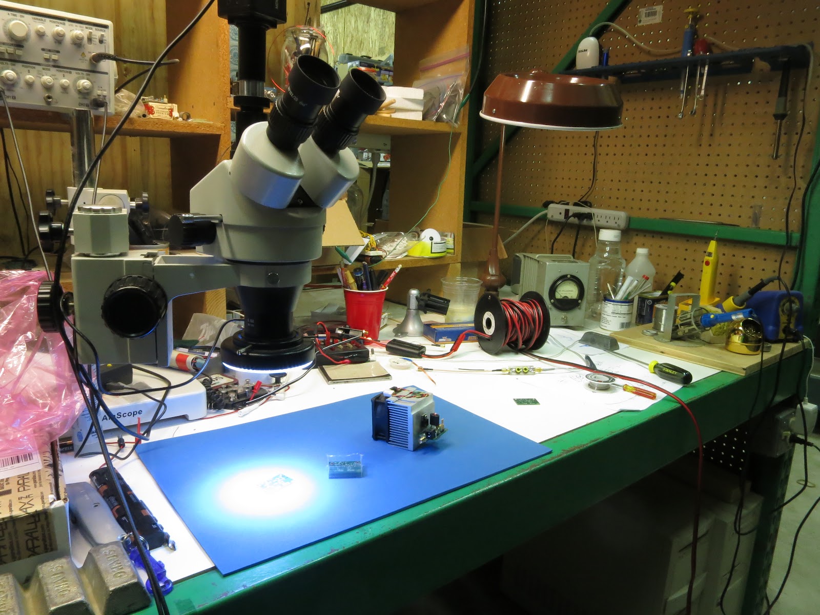
The Bench
Dishearted - I gave up - left the shop "without" putting away my tools and cleaning up (I normally always clean up before leaving).

Bummer!!

Several days have past (about a week), it is now Sunday and I am planing to go to Jack's Homebrew Club evening meeting on Tuesday, and the following night I am going to the pQRP monthly meeting. I decided to clean-up the PA (to remove excess solder flux) to make it "look good", and take it to the two meetings, to show my epic FAILURE of a nice idea for the PA.

While cleaning the circuit board, I noticed one of the legs of the (necessarily) "dead bug" mounted transistors did NOT appear to be soldered (with filets) to its pad, it appeared to have just a glob (flyspeck) of solder on the bent leg. This was the drive transistor for the output power FET, maybe it was not actually soldered down!!

For me, it is actually quite difficult to see a single SOT-23 pad without a Microscope.

Under the Microscope I could see it only had flux between the pin and pad!! I heated the soldering iron, fixed the joint, re-connected the Propeller Beacon Exciter, the output Low Pass Filter, the 50 Ohm Dummy Load, and the 12.6 Volt supply, . . .

WOW!, I observed 43 Volts PP at the load. That is; (43/2*.707)^2/50 = 4.7WATTS - YES!!!!!

Which is a gain of 25.93dB.

The PA-47 Curcuit with a Sziklai Pair Driver works!!

I installed the rest of the TR circuit and Relay on the under side of the PCB, but - DANG! The relay would not work! Now what??

After several hours, I discovered that I had attached the Relay Coil to the opposite pins on the Library PCB pads within DipTrace, the Relay is polarity sensitive. Like the drive transistors I had jury-rig the Relay by cross wiring the coil under it to make it work (the fix can not be see in the photo).

After cross-wiring the coil pins and re-installing the Relay - All worked as expected :-)
PA-47 - With TR Circuit and Relay Installed
Regardless of Success or my Failures, Tess is always watching, to make sure everything is being done right! She was not involved with the PA design or PCB layout, but some how she must have missed the poor solder joint!! (actually, . . . she is watching her ball that I placed on the bench :-). If I had her concentration (and other admiral attributes), I may have NOT missed the above critical project details :-))))

Tess - Doing Her Job,
Production, Test, and Final Inspection
I am , . . . ah, . . we are NOW both Happy Campers!

. . . . . Tess has her Ball, and I have my PA!

I will later post more PA-47 Project details. More testing, and more work is needed to install angle brackets to support the PCB.


UPDATE:

Increasing the DC supply of up to 14.2 Volts (via a heavy duty Lead Acid Battery on a Charger), I got 60 Volts PP at the 50 Ohm Load, (60/2*.707)^2/50 = 9.0 WATTS- Nice!!

Note to self:
A Fan control via the TR circuit or HeatSink Temp would be useful, it would save some power and would be quieter.

UPDATE:

Here is the PA-47 running on Jack's Bench at his Homebrew Club meeting, the photo was taken by Jack and who suggested this photo would make a great (complex) puzzle picture :-)
PA-47 Running on Jack's Bench

--

Monday, November 26, 2012

PCB Solder Jumpers - Cont'd

For Diptrace my new (proposed) Solder Jumper (see previous post), the buried trace connection point on the pad was created by creating the "shape" with the "initial point" at the desired connection point. The "initial point" is where the construction of the "shape" starts and ends. After construction, the "shape" is converted to a "pad" via a right mouse menu item. Below, for demonstration, the "initial point" was artificially exposed by opening (moving) the adjacent points at the left. The grid is set to 2 mils.

For Demonstration the Trace
Connection Point is Exposed at the Cursor

Normally, the gap would be closed, and the two (moved) points would be located at the same point.

This use of the "initial point" may be documented some place in the Diptrace manuals, but I have not found it.

--

Saturday, November 24, 2012

PCB Solder Jumpers

I have received some good feedback on Patterns for PCB Solder Jumper (see previous posts).

Experiments with very small 0201 size foot prints were NOT as successful as I would like. The small 0201 pads would not hold enough solder to allow proper bridging of the gap between pads. A usable bridge could only be made with very dry slaggy solder.

I am trying the new Solder Jumper Pattern as I suggest in the previous post. Here are the proposed dimensions, the folded pads should help hold the solder and aid in bridge creation. Or, at least that is the plan.
Overall size is 72 x 32 mils (0703)
Dimension Values Shown are Mils
The trace connection is a point within the thicker section on each end. Finding the method of creating that point was via trial and error. Diptrace uses the first created pattern point as the attachment point, I had to artificially bury the point inside of the pad to make trace connections easy.

The PCB Manufactures that I use, and my own Homebrew PCB processing, should be able to create the pattern without difficulty.

I have recently sent a small board off to Manufacturing with one of these new Solder Jumpers ,  Soon, I will report the results.

--

Thursday, August 2, 2012

I am Impressed !!

I am Impressed with the new DipTrace 2.2.9 Beta !!

I have been working in my Shop the last few days, installing a Vacuum System to remove Saw Dust and help with general clean up. While taking a short break, I sat down at the computer to read some e-mail.

I just received an automatic e-mail from the DipTrace Development Crew, that  stated DipTrace 2.2.9 Beta was available for download.


Because I use DipTrace for most of my Homebrew or Manufactured PCB's, I was anxious to try the new version. My short break turned into several hours - I was trying all of the new Features and Fixes to problems (that bothered me until now).

I am impressed, the DipTrace Development Team has fixed many of my concerns.

The Beta Fixes make PCB's very easy now; To move a trace - click on it and move, to move a VIA - clink anywhere on it and move. New users will find PCB edits very-very easy and obvious.

My DipTrace Survival Guide has becoming much less relevant, I have updated the Guide with the details that I have learned so far, more to come.

Thanks for the Beta, Guys.

--

Wednesday, April 4, 2012

Encouragement from DipTrace

As an addendum to my DipTrace Survival Guide, the following is my email exchange, which can be found on the DipTrace Yahoo Group List, at:


Note: As can be seen, plans are in progress to help make PCB layout easier.


Hello

After completing the schematic capture, and now on PCP layout, how can I avoid the edit mode changing to "Rat Line" mode?

My schematic is complete and do NOT need any Rat Line additions or deletions, but it seems that the default edit mode is "Add Rat Line", even though all I need is to move parts, add or modify traces to build the PCB layout.

Having the mode switch to "Add Rat Line", when a pad touched is very-VERY irritating. The default mode should default to the last that I set.

If the default edit mode could be fixed, I would be a happy camper!

Regards,
Eldon Brown


Hi Eldon,

If you want to move a component, move mouse pointer over the component and left click to select it. It is important, that component will be highlighted in green color. If you see red highlight, program will switch to "Rat Line" mode. It triggers automatically, but we plan to add separate button for switching in "Rat line" mode.

You can also disable editing net structure (Route/ Lock net structure) to prevent wrong connections.

Alex Mihailenko
DipTrace Team


Alex,

Thanks for the encouragement, but,. . .

I deal with very small, very high density boards where many components overlap, and multiple via's are often contained within a component outline. Clicking on a component without inadvertently selecting a pad is problematic (especially SMD's). And therefore, in my experience, changing into "Rat Line" mode happens VERY often, which requires YET another attempt to re-set the mode to do the task at hand (with many wasted mouse clicks).

Also, "via's" are the worst offender, trying to move a via is always unnecessarily difficult (there must be a better way that I am missing). Each time I click near a via, the mode switches to the unwanted to "Rat Line" mode. To move a via, I have "learned" to very carefully click on one of the four, very small "magic" spots around the via (at 3, 6, 9, and 12 o'clock positions). Otherwise the mode switches to the unwanted "Rat LIne" mode, again :-(

Note: as per you reply:

>> It is important, that component will be
>> highlighted in green color. If you see red highlight, program will switch
>> to "Rat Line" mode. It triggers automatically

Maybe if that logic was reversed all would be well.

Anything new, developments, quick fixes, updates, or training tips, to address this problem will be greatly appreciated by myself (and maybe others).

Thanks.

Regards,
Eldon Brown


-

Wednesday, March 14, 2012

Prop TCVCXO PCB

I have been watching/testing the 10MHz TCVCXO that I installed to replace the master clock on the Propeller (see previous posts). The stability is better than I had hoped, but the installation was NOT as good. I just soldered the TCVCXO onto the Propeller Protoboard where pads were available, but spacing was not optimal as solder bridges where necessary to make it fit. It was a jury-rig just to do some initial test.

Now that I had time to think about how it should be mounted, I decided to build a small PCB to hold the the parts; TCVCXO, by-pass cap, two fixed resistors, a variable tuning resistor, and a output cap.

Schematic on CircuitLab
Keeping with my on-going project goal, I wanted it to be as small as my ability allow. The results was a PCB that is 0.453 inches by 0.492 inches. The circuit will stand on three legs/pins which insert into mating sockets. I installed the sockets on the Prop Protoboard using existing holes, which provide 3.3v, ground and the clock input.

If the TCVCXO can not to be used, or if I want to use the original crystal, it can be re-inserted. Only the three pin-sockets were necessary and they can be abandoned.

DipTrace Layup
I will have the board made by a commercial PCB vendor, but for a quick test, I resorted to my tried-and-true Toner Transfer Method.
Circuit at Different Stages of Toner Transfer
I made more than one copy, Just in case Murphy was Watching

Components Loaded and Ready to Install
Some things just looks Ugly, when you get TOO close.
The TCVCXO PCB,
Two Fixed Resistors and Pot in Foreground
10MHz TCVCXO Center
Two Cap's in at the Far Edge
Using the board, is just a matter of changing the clock parameters and plugging the TCVCXO in.
TCVCXO Installed on the Prop Protoboard
It Sets Just Below the Edge of the LCD
I was easy to do, and it works GREAT!

--

Sunday, December 4, 2011

DipTrace Survival Guide


DipTrace Survival Guide

Compilied From My Use and Observations

By: Eldon R. Brown
Dec 2, 2011
Update: Aug 2, 2012 - DipTrace 2.2.9 Beta
Updated: Aug 12, 2015 - DipTrace 2.9 Beta


Update - Aug 2, 2012: Note I have not explored all of the Changes provided with DipTrace 2.2.9 Beta, I will make further correction/additions as I experiment. So far I am pleased with the progress - Hats off to the DipTrace Devs.


I have been using DipTrace for several years and have recommended it to many new users. Most of the projects, Schematics and PCB's documented within my blog have be created with DipTrace. This Survival Guide it a collections of my Opinions, Use Tips and Techniques.


I will try to Expand and Update this Guide, as new software revisions are released, and when I have time. Occasionally I will repost this, when signification changes are made.


The main reasons that I use DipTrace are:
  • Ralative Easy to Learn
  • High Resolution Cross Hatch Copper Pour
  • Consistent High Quality Exported Gerbers
  • DipTrace Runs on MS, and Linux via Wine (Linux is a must for me)
  • Low Entry-Level Price
  • Easy to Edit Traces - Added via DipTrace 2.2.9 Beta


The few things that I DO NOT LIKE about DipTrace:
  • Library Management and It’s Use is Miserable!
  • Automatic Edit Modes Always Picks the Wrong Defaults - Fixed DipTrace 2.2.9 Beta
  • Lack of User Defined Softkeys and Macros - Partly fixed in DipTrace 2.9 Beta
  • Lack of Project Management Tools, and the Hard Coded Internal PATH to Related Schematics contained within the PCB file makes it difficult to; move or archive related design files.
  • Auto Route does not use the same grid that Manual Route user has access.


The following are my Survival Suggestions and Observations learned while using DipTrace.

  • There are only four magic spots to select and move a VIA, they are at the 3,6,9, and 12 O’clock positions. The magic points are slightly off of the pad, experimentation is necessary to find them. - Fixed DipTrace 2.2.9 Beta
  • To select the Ground Pour, you must select it only at the edge, even though it appears on large areas of your PCB.
  • To update a part Pattern on the PCB layout,
    • Clone (or obtain) a new pattern into you private Active Library
    • Edit and save the Pattern as necessary
    • Edit and save the offending part within your Private Active Parts Library
      • Attache the modified Pattern to the part
    • Delete Connections from offending Part within you Schematic
    • Insert a the new part into the Schematic
    • Connect wires as necessary
    • Save the modified Schematic
    • Edit the PCB
    • File -> Update From Schematic ->
    • Reposition (new) modified part as necessary
    • Reroute Part Connected Traces as necessary
  • With very small traces and parts it is sometime necessary to move the part to access underlying traces. - Fixed DipTrace 2.2.9 Beta, The Trace Edit mode does not change when clicking on a trace under a part.
  • It is best to do hand routing, as the auto router does not use the same grid as you have access, therefore it will be difficult to make small change and make your circuit consistent.
  • When doing route modification, Rat Line additions has highest priority. There constantly watch and reset “trace modify” mode as necessary. The mode does not stick. - Fixed DipTrace 2.2.9 Beta
  • You may find it difficult to consistently move a board point, the priority mode is “point addition”, press “CTL-Z” as necessary to remove the unwanted point.
  • Due to the lack of custom softkey, many tasks such as “un-Route Trace” and “Auto Route Trace” can be found in the right click menu, but the two menu items are not next to each other, and therefore you will need to learn the menus.
  • To avoid trying to fix a difficult routed “Trace” it is sometime easier to create a second (and simpler ) manageable trace before deleting the original. - Fixed DipTrace 2.2.9 Beta - Edit mode stays set
  • When moving parts on the PCB, remember that the mode often switch to “Rat Line Add” mode, “Escape” will return you to part select mode. This happens often, therefore for speed you should place your left hand (hover) near the Escape key. - Fixed DipTrace 2.2.9 Beta
  • Lock Net mode does not avoid the “Net Add” process, it only increases the clicks and dialog to escape from - i.e, a net productivity loss. - Fixed DipTrace 2.2.9 Beta - No longer a problem
  • The supplied Pattern and Part Libraries as difficult to “Brows” and therefore if you do not know the nomenclature use in the library of a spacial part, it is sometime much easier to create your own part. Simple standard parts are sometimes very difficult to find, for example try to find a 3-pin FAN header. - Many more parts in DipTrace 2.2.9 Beta, more investigation need.
  • The default mode for both PCB and Schematic is to add parts from the active Library, be careful not to to add unexpected hidden parts. Here again, pressing the Escape key often generally avoid the problem.
  • Because DipTrace does not maintain a Schematics and PCB’s as a project, and because it has Hard-coded Links from the PCB back to the Schematic, It is best to plan you project directory structure before starting.
  • If you move a Project (Schematic and PCB files) remember the Hard-coded links will still point to the original directory space. Modification of the links in the PCB files can be corrected by “re-associating” (updating from Schematic by Reference”. Or if you are clever, and do not mind “text” editing the PCB source file, the Hard-coded link to the Schematic can be change.
  • For easy access to your private Library of Parts and Patterns, move your library to the top (and which is left) of the LIB list. Note there is not an easy way to move the appended (bottom of the list) Library except one click at a time for each library in the list (actually it takes two clicks, one to select and one to exchange adjacent Libraries). It may take several minutes to move a library from the bottom to the top. Avoid the problem, put your Library at the END of the list, as default for an added library, just remember where to look.
  • Component placement rules do not appear to observe a shortest trace placement strategy. Many times two schematic parallel parts will be place with crossed nets. Also, Power and ground nets can not be ignored for auto placement.
  • A useful strategy for manual placement, is to hide the Power and Ground nets, place adjacent schematic parts together, move them into position as a group. 
  • Do not modify PADs on the PCB, an update from the Schematic will remove your changes. Modify the Schematic Parts with the Correct PAD information for the Project.
  • There are about 2500 3D parts within one single (file system) directory, take a hour (or two) to sort like parts into sub-directories for easy and quicker access (accessing or just listing the directory repeatedly takes a lot of CPU time).
  • The Schematic and PCB Title Options only includes two automatic fields; “file name”, “sheet name”. Other useful information must be manually included, for example: “Date last updated”, “Project Directory Name”, “Revision Number”, “Creator or Editor Name”, default “Company Name”, “Related Schematic file Name”, Pins Used, Layers Used, etc, etc.
  • For Documentation, each time Print Review is used the options must be re-setup, options are not saved from previous use.
  • Before having a PCB created, it is best to verify each of the Schematic part’s Attached Pattern. Because the Pattern is not one of the “optional” labels that can be printed on the Schematic, it is necessary to inspect each part’s Properties, or right click on each and then click on “Attached Pattern” and change it as necessary.
  • DipTrace does not support "Targets" for assistance in Top and Bottom layer alignment. A useful Technique is to use circuit "Edit -> Panelizing" to print extra copies of the same circuit for alignment images, a 3 by 3 panel provide corner images for the single center image alignment.
  • As Time Permits, I will update this with more DipTrace Survival Tips.

UPDATE:
A very nice tutorial has been created by a user on the EEVBlog Forum, See: http://goo.gl/bMp6m

DipTrace 2.2.9 Beta is available at http://www.diptrace.com/downloads/dipfree_beta.exe


--

Monday, October 24, 2011

Teensy Programming Shield

Jeff - KO7M and I have been working on several Arduino and Teensy projects, to control QRP and Beacon Transmitters. To expand and progress to the point where we will use raw chips in planned projects we decided to produce a Teensy Programming (under) Shield. For several projects we have used the Teensy as the development platform.
As Designed in DipTrace

The Teensy will plug into the top of the Shield. After several iterations and corrections of schematic I we have a layout.

Today, I used the Toner Transfer Method to create the board. High resolution two sided boards are tough but they can be done. The Teensy Programming Shield is .75" x 1.75" with 8 mil traces.

Etched and Ready for Inspection
There are not many traces so it was not hard to route or build. If I had need for more than a few boards I would have sent it out for FAB.


The Etch Looks Good
and both sides look like they are in good alignment
These are 8 mil Traces, and 6 mil Ground Grid
After Laser Toner Resist is remove, the board is cleaned and polished, and then placed into a small dish of Tinnit. In about 5 minutes the board is bright and shiny.
Tinnit was used for Tin Plating
Tinnit works well, with good coverage,
but it is very thin (.004").
The Results:


Parts Loaded
Double sided HB board are difficult as the socket pin are typically used to transfer the traces between sides and therefore both sides of the socket pins require solder. With care this can be done by raising the socket a small amount and soldering with a very sharp iron. Also, small errors of alignment between the image of each side make for difficult drilling and therefore pad are not always centered on the component pins.

Cut, Drilled and Parts are loaded, in this case Headers and one jumper.

Ready to Use !
As you can see the Header were raised about 1/10" to facilitate top side soldering the few pads which are connected via traces. Raising the parts would not be necessary if this board was from a FAB shop, plated through holes would make loading parts much easier.

In use, the Teensy will cover the first 24 pins (far end), short jumpers will be used if need for the none standard Teensy pin locations. For ISP Programming effort, only one jumper will be required - the RST pin.

With the Teensy plugged in hopefully there will be enough space to plug in the programmers? To use the Shield to program the Teensy, a short jumper is still needed between the RST pin (on end of the Teensy) and the third pin on the near open socket holes. That hole, is connected to the RST pin on the 6 pin Programming Header. We could have included dedicated RST pin and socket as part of the Shield, but that would require we alter the Teensy with a dedicated pin, disallowing it to be used directly with simple circuits on protoboards.

The Teensy is Installed, Ready for Programming,
It can be used
In or Out of a Protoboard
Now it is time to do some Direct AVR Programming - Jeff!

--

Wednesday, June 1, 2011

AutoDyne Receiver Project

I have been working with "virtual" electronics for the last few days. I must have inadvertently turned a corner without me noticing. I have not been in my Shop for days, most of my work has been at the computer in the Loft.

In the past, I have always breadboarded my circuits before creating Homebrew PCB's, which I think is still a good idea. But, professionally manufactured PCB are so cheep, that I decided to skip the breadboard stage, with the idea that I can re-do-it if the circuit fails miserably.

Normally I would not Blog about a Project until it is successful, but for this project "you are going for a ride", and you will see the success or maybe a total failure.

My current little project is to build an "AutoDyne Receiver", as documented by Nick - WA5BDU and describe at Wikipedia.

This circuit is a Frequency tracking receiver that outputs the station audio for a speaker circuit, and the RF carrier frequency. If it is configured to receive WWV (say at 10MHz) the RF output can be used for a frequency standard (or at least that what it says in the documentation).

This circuit was originally constructed with discrete transistors, and then with a CA3046 Transistor Array. But, the CA3046 part is currently almost unobtainable (it must be made of unobtainium :-), I will substituted with five SMT 2N3904's.

This is what I have so far, note the circuit has been redrawn in sections, and parts from my junk box have been substituted where necessary. Refer to the original link above. I hope I have not miss re-creating the circuit.

The AutoDyne Receiver Circuit in DipTrace

Proposed Circuit PCB - 1.6x.9 Inch

A DipTrace 3D View

As with all of my HomeBrew PCB Circuits I have tried to make this board as small as possible, is will be 1.6 x .9 inches and will be powered initially by a 9 Volt Battery (if you know my projects, what else would you have expected?).

The PCB is now on order. If all goes well, my small board with be merged via DorkbotPDX onto a large manufacturing board on Jun 6th, and then enter their normal manufacturing process. My board(s) should be returned around Jun 15th.

This little project has been on my drawing board for more than a year, only recently have I pushed it along to the PCB stage, my original planned implementation used much larger parts. Now, I will use small 0805 and 0603 SMT parts. After looking at the photos above, I could have (with more work) held out for an even small build/design. A lot of space is taken up by the Audio connector (lower right on PCB)?

Later, I will report the results (or failure) of my attempt to skip the Breadboard stage for this project.

Again, Thanks to Nick - WA5BDU for documenting (and his mods) of the original circuit. Note: many others have had their hand in the circuits creation. The link is an interesting read.


--