Friday, December 28, 2012

PA-47 at High Power !

The little Class "C" PA-47 RF Power Amplifier has grown up, I have doubled the original output of 4.7 Watts, to greater than 14 Watts.
PA-47 Ready for Modification
The new FET Leads will be bent
to Accommodate the Existing PCB Holes
I have replaced the general purpose IRF510 Power FET with an actual Special Purpose RD15HVF1 HF Power FET (from RFParts), and then connected the PA to a large stable DC Supply (Battery).

The results at full power, are;
  • With a 12.51 Volts DC supply running at 2050 ma (25.7 Watts DC Input with FAN)
  • Exciter provides 12 mWatts Input at 10.140MHz
  • The PA-47 output is 75 Volts PP RF measured at a 50 Ohm Load, which is: 14.1 Watts
  • The HeatSink Temperature at the FET raised about 20 degree to 94.7 Deg F
This is a gain of 30.70dB and a Efficiency of about 66%.

I am a real Happy Camper !

Note: this is a very small 1 x 1.5 inch PCB, with a large CPU HeatSink.

-

I plan to re-layout the PCB to accommodate a Fan Control circuit and correct the small layout errors as explained on previous posts.


--


Wednesday, December 26, 2012

Destructive Testing of PA-47

Late last night before leaving my Shop, I inadvertently put a 12.6 Volt supply plug onto the 1 Watt PA, which was designed for only 9 Volts (see previous post). The results was a toasted 2N7000, but that is NOT really a problem, as I have replacement parts (and boards).
PA-47-1 and PS-47-5

Later in bed, and while trying to fall asleep, I got to thinking; Why not do some Deliberate Destructive Testing while recording circuit parameters? I could think of several scenarios that would be fun to try.

And besides, how often do you get to deliberately abuse two of your favorite RF Power Amplifiers?

Some Abuse Comes to Mind:
  • Put an over-voltage on the supply connector (similar to the mistake above).
  • Run the PA at the over-voltage condition while cooling the FET with Freon.
  • Create maximum VSWR at the PA output with a shorted and open coax (this may have to wait for another day) 

For the tests, several FETs were prepped from randomly selected Volunteers. Each was outfitted with an attached HeatSink. The HeatSink is a 1 inch square piece aluminium flashing, super-glued to the FET.
Preparation for Expected Failures
Initial Normal Use - Base Line Tests

Input to the amplifiers is provided by my Propeller microprocessor system, which supplies about 12mWatts into the amps (see previous posts).

PA-47-1, A one Watt PA, with Normal DC Supply Voltage
  • Power Off - HeatSink at 75.7F
  • 9.1 Volts DC, RF input Off, 41 ma, HeatSink at 82.4F
  • 8.8 Volts DC, RF input On, 250 ma, HeatSink at 103.6F => 20 Volts PP at 50 Ohm Load => 1 Watt
PA-47-5, A Five Watt PA, with Normal DC Supply Voltage
  • Power Off - HeatSink at 73.4F
  • Fan Off, 12.1 Volts DC, RF input Off, 90 ma, HeatSink at 82.9F
  • Fan On, 12.1 Volts DC, RF input Off, 270 ma, HeatSink at 73.8F
  • Fan On, 11.5 Volts DC, RF input On, 1170 ma, HeatSink at 102.9F => 42 Volts PP at 50 Ohm Load => 4.4 Watts

PA Input (lower) and Output (upper)
Output is 4.4 Watts
5 Volts Per Div

Destructive Tests

PA-47-1, A one Watt PA, with Over Voltage Supply - Rated at 12.5V at 1200 ma
  • Power Off - HeatSink at 75.7F
  • 12.1 Volts DC, RF input Off, 80 ma, HeatSink at 84,9F
  • 11.8 Volts DC, RF input On, 710 ma, HeatSink at -25.3F with Freon => 30 Volts PP at 50 Ohm Load
  • 11.8 Volts DC, RF input On, 520 ma, HeatSink at 148.6F without Freon => 25 Volts PP at 50 Ohm Load
  • Output Transformer was Hot to touch.
  • Only the FET Failed 40 seconds after Freon was removal, afterwards maintained 145F while power was applied - FET was toast!

PA-47-5, A five Watt PA, with Over Voltage Supply - Rated at 31.5V at 3170ma
  • Power Off - HeatSink at 73.4F
  • Fan connected to a separate 12 Volts DC Supply
  • Fan On, 30.19 Volts DC, RF input Off - The FET and the two drive (Sziklai) transistors Failed within 3 seconds of DC voltage being applied.
End of Destructive Testing

The Dead Soldiers

Several FETs were used to collect this data, only a condensed synopsis is provided above.

Conclusion

The PA-47 Circuit boards survived much better than I would have had imagined, components failed long before the PCB traces. For Higher Power PA's more design aspects need to be understood and considered.

The two PA circuits have be restored to there former condition, awaiting further tests or use.


Destructive Testing - Epilogue :-)

For the above described Destructive Tests, all intentionally destroyed FETs were randomly selected Volunteers (RIP). They are well preserved and available for additional photos and future forensic examinations.

Although mildly inconvenienced, no Electrons were Captured, Created or Destroyed as part of these experiments, they were ALL returned to their point of origin.

Almost all (well, maybe some) of the released Magic Blue Smoke was captured or contained for return to the part manufacture, if desired.

All transferred RF energy was absorbed by the 50 Ohm Load, most of it was emitted as therms and dissipated into the surrounding area. Only a small fraction of RF energy was transferred to a local Receiver where is was used to monitor the testing progress.

Only Ozone Depletion-Free R-134 Freon was used for the cryogenics phase of these tests.

With some microscopic surgery, all Causalities were fixed, repaired, or replaced. Both boards have fully recovered and will be returned to original service.

All of this was in the name of; Science, Ham Radio, and/or just plain FUN :-)

--

Sunday, December 23, 2012

PA-47 At Only 1 Watt

Original PA-47
with Large Heat Sink, 
Matching Transformer
and FET IRF510
In keeping with my goal of making my Homebrew projects as small as my abilities allow and using the same previously created PCB board (see previous post on my PA-47 Power Amplifier)

I have reduced the size of the output matching transformer and changed the output FET from a IRF510 (TO-220) to a 2N7000 (TO-92).

New PA-47  Running at
1 Watt Output

Knowing that the 2N7000 would not produce the same 4.7 Watts of the replaced IRF510 with its large heat sink, I planned to reduce the supply voltage; from 12.6 Volt down to 9 Volts, and reduce the size and turns ratio of the matching transformer form 1:3 to 1:2.


New Replacement Parts
of the Original PA-47
are the 2N7000 and 

Smaller Matching Transformer

Initial test produced 1 Watt RF output, and a Very Hot 2N7000 FET. A small 3/4 inch sq piece of aluminum flashing was super-glued to the FET which solved the heat build-up problem. Just in case, I also installed a pin socket for each leg of the FET (which means I can easily replace the FET, if I inadvertently cause it to release its Magic Blue Smoke :-).

For this first test, the DC input was 8.5 Volts (not a very fresh battery set) at 360 mAmps: or 3.06 Watts DC Input, which suggests the PA at only about 32% efficient (more work is maybe needed to increase this). The standby current (no RF input) is about 13 mAmps, and most of that is used to drive the green Power-On LED.

30 Meter Low Pass Filter

Without the FAN and Large Heatsink that was used in the initial PA-47, this PA is silent.

Like the original PA-47 an outboard Low Pass Filter is necessary and was used for this experiment.


TR Relay Mounted Under the PCB

The yellow-tag jumper on the header turns on the TR Relay, which is mounted on the under side of the PCB. Normally transmitter control from the exciter would be connected to this header.

The RF voltage measured at the 50 Ohm Load via the scope: 20 Volts PP, (20/2*.707)^2/50 => 1 Watt, or as per the web  RF calculator.

This smaller and lower power PA will be perfect for my ongoing Propeller 30 Meter Beacon efforts.

After I correct the PCB layout (see previous discovered errors),  and if there is interest, I may make the PA-47  board available, or as a complete Kit (but, as a board or kit, this would not be suited for first time builders, nor a builder without a Microscope).

The Exciter (Driver)
The Exciter
Outputs 12 mWatts

For this experiments and as explained previously, I used my Propeller Transmitter as the exciter which provides 12 mWatts of drive. The Propeller is the second board in the stack.

--

Wednesday, December 19, 2012

CNC - Projects

I know this post is not about Ham Radio, but . . .

At Jack's Homebrew Meeting
Jack, Bob and Walt
One of the many topic of discussion at Jack's Homebrew Club meetings last night, one was his Homebrew CNC project. He has used his CNC to cut Wing Tip molds for a Boeing Aviation Restoration project.

Also, I have been discussing and following John Hoaglun progress of his recently acquired CNC PCB Router. John has done some interesting experiments to create configurations that allow for detailed routed PCB projects.

All of this has rekindled my interest in my own, all most completed (75%) Homebrew CNC Plywood Router project - which I named the "M45".

M45 has been standing in the corner of the shop for several year, gathering a little rust, waiting for the right moment to be reactivated. If I remember correctly, the bed was designed to hold a 4 x 8 foot sheet of plywood, with an active routing space of 4 x 5 feet.

All of the parts for M45 were cut on my PlasmaCam CNC Cutter, Welded together, Milled, or folded in my shop. Motors, Transformers and some other Electronics were purchased from Surplus Center. The actual motor controllers are from Geokodrive. I added my own designed positions encoders to the motors.

The X and Y feed motors are quite heavy duty DC motors, I do not remember the spec's. They are about 4.5 inch diameter, about 8 inches long, and with a 5/8 inch shaft.

Y-Axes Motor and Drive Chain
X-Axes Motor and Drive Chain
The Z feed motor is smaller, with an internal encoder. This part of the project needs some rework to center the feed screw on the vertical carriage.
Z-Axes Motor (with internal encoder)
and Drive Belt

The Y gantry rolls on bearings at each end of the slide, and attached to a self tension Chain and Cable. An under slide bearing provide stability.
Y-Axes Drive Chain and Pulley

Y-Axes Rail
The Chain and Cable are self tensioned, the carriage attaches with a single bolt (one each side). The other rail looks the same.
Y-Axes Chain  and Cable Attachment

Under Slide Bearing
Tension is provide via the bolts on the ends
The Controller uses three Geckodrive Motor Controllers as seen on the left, the Power Supply and Transformers as mounted on the bottom. Four sets of Transformers and two sets of Rectifiers are paralleled to supply voltage to the large filter Cap. Rectifiers are mounted low on the front (right side), Controls and Switches upper right.
CNC Controller and Power Supply
Fuses and individual motor controls (i.e., On/Off and Jog) switches and status lights are on the front.
CNC Controller
Some un-used parts :-)
Un-used Motors
These were tried, but too small for this Project
They maybe used for another CNC project
About the only things that are missing to complete the M45 project are; the Wiring Harness, the Vacuum System, and some rework on the Vertical Feed. Note: This project was started long before I knew much about CNC.

As shown the Motors are mounted, and the Controller has been built and tested. The project was put on hold for a variate of competing interests and responsibilities.

I should complete this Project.

But alas,  . . .  I have too many projects, and too little time (now that I am retired :-)  to (re)start work on another project

I wonder, . . . How did I ever get anything done when I was still working a 60 hour per week job???


--


Tuesday, December 18, 2012

PCB/Vinyl Cutter

Hey, I just saw a Great Post and Idea on the "Homebrew_PCB" yahoo list by Richard D.

I want to capture the idea here for my later reference.

It is a Roberts Quik-Cut Vinyl Tile Cutter that can be used to cut PCB material

It can be found at Home Depot

  • Model # 30002
  • Store SKU # 729019
  • Price: $50


I will have to try one of these.

--

Monday, December 17, 2012

PCB Solder Jumpers - Cont'd

With the success of my previous PA-47 project, I feel like blogging again.

Previously, I proposed a Solder Jumper Pad Footprint for my future projects (see previous post). One of those was used on the PA-47 Amplifier. The manufacture did not have any problems creating the pads, as shown.
Solder Jumper - 0703

The overlapping hooks of the jumper pattern makes for easy filling with solder, and then with some Solder Wick, it was just as easy to re-open.

Solder Jumper - with Solder
I may need to create a larger jumper pad set for larger traces, as shown the traces between pads are 16 mils. For reference, the copper pour ground grid is made with 6 mil traces.


A Personal Note: This post is a milestone for me, it is my 100th post for the year, which is more than any previous year, and far more than I would have expected when I started in 2009.

I suggest everyone start a Blog. It is very enjoyable and you will meet and network with many interesting people. I would also suggest you encourage your kids to blog (ether privately or publicly) about topics that interest them. Kids with learning-disabilities should start ASAP, even if they only write one line of text each day - they WILL see progress. Because they will blog about topics of their interest, and because they are the expert of their activities, it will be an easy task. They may not be a potential Doogie Howsers, but blogging will help collect ones thoughts. In the TV show plot, Doogie was a great Blogger.

Actually, my blogs are not for me, not for you, nor any of my current readers, my blogs are for my Great-Great-Grand-Children - it is a way to communicate with them of my ideas, interests, and thoughts. I would have loved to have found letters (or blogs) written by my Grand Parents, or their Parents.   Sadly, I only know the names of six generations of Fathers, and very little else.

Do your part - Create a Blog!

--

Sunday, December 16, 2012

PA-47 - A QRP KiloWatt

I have not posted anything for the last few weeks, I have been a little bummed out.  I started work on an interesting Project, which is a "QRP KiloWatt", a 5 Watt Amplifier. It will be used with my Propeller Beacon Project (see many previous posts) and maybe my other QRP projects.

Sziklai Pair
What renewed my interest in building yet another PA, was a new (new to me) configuration of transistors - called a "Sziklai Pair", or sometimes referred to as a "Complementary Darlington". The configuration is actually quite old, and was invented by George C Sziklai  (pronounced as: "SICK-LIE", which is the best guess as per the web). I had not seen or used the configuration before.

To me, the interesting spec is that the Sziklai Pair can produce nearly Rail-to-Rail output voltage - which is exactly what is needed for a FET PA driver. FET PA's require high signal voltages (i.e., +6 or 7 volts to drive the gate) which is much more than the typical 0.6 volts for a normal transistor. Transformers can be used to produce the high drive voltages for FET PA's. But, I did not want to do that, especially if two simple transistors can do the task. I have built PAs before and always had messy drive circuits and problems.

I configured my planned Sziklai Pair Driver and FET circuit within LtSpice. It took a while to get the configuration and front-end bias right for my desired "class C" operation. But in the end, it is much simpler than I had imagined. Resulting in a circuit with very few components. LtSpice suggested I should get about 4.7 Watts at 10.140MHz from 12.6V DC when driven from my Propeller (Prop) Beacon, The Prop only provides about 2.5 P-P Volts at its output pin (or only about 12 mWatts drive).

Excitedly, I transferred the LtSpice configuration into DipTrace Schematic Capture, and from there created a DipTrace PCB layout. The circuit includes; SOT-23 2N3904 and 2N2906 for the Sziklai Pair, a IRF510 for the PA (standing up to mount to a heat sink) and a TR Relay and its support circuit. As usual, I wanted the circuit board to be as small as my abilities allow. The PCB was going to be only 1.5 x 1.0 inches, using SOT's and mostly 0603 parts.

While designing the circuit, I noticed that I had used mostly "47" valued parts, for example 4.7K resistors and 47nF capacitors. And, therefore I decided to name my new QRP KiloWatt - the "PA-47". Just for fun, and with very little work, I was able to convert all parts to 47 values. Besides, LtSpice said it would produce about 4.7 Watts - so what else could I name it?!!

The circuit was so simple I decided NOT to try to breadboard it, I just quickly pressed the DipTrace button and ordered the PCB's (that is way too easy).

For about a week and half, I waited for the PCB's to return from the Manufacture.

PA-47 - PCBs as Received
PA-47 - PCB Under the Microscope
Finally, the PCB's arrived, I excitedly loaded a board. But - DANG!! - I noticed I had used the wrong SOT foot print for the two Sziklai Pair transistors!! Maybe I pressed the DipTrace Order button too soon (the button is just too easy and handy). The two driver transistor's Emitter and Bases were exchanged on the PCB - DARN, DARN and DANG!
2N3904 SOT-23
as  MMBT3904

OK, now what, . . . . if I turn the transistors up-side-down, "dead bug style", the PCB foot print would work. All I had to do was bend the legs up and then try to solder the SOT transistors up-side-down on to the PCB. I notices the leads almost broke off when bending them back that far. I planned to fill the little crack with solder as part of the installation process, it would only require a slightly larger glob  of solder on the pin (actually the glob of solder is about the size of a flyspeck and can only be seen under the Microscope).


For the initial tests, I would not install the parts for the TR Relay Circuit, as it was not really necessary (I just shorted two pairs of the pads together, as if the Relay was always on).

PA-47 - Mounted to a CPU HeatSink
Output Matching Transformer and Connector
on the Right Side
PA-47 - DC Power and RF Input Connector
on the Left Side
I connected the Propeller Project as the Exciter, a Low Pass Filter, the 50 Ohm Dummy Load, and the 12.6 Volt supply to the PA, the Fan came on (a good sign)!. The Propeller was outputting its 2.2 Volts into the PA input. . . . . But nothing was coming out of the PA, - more Dang!

I spent the next several hours trying to figure out the circuit or problem. Remember is a NEW untried circuit, and there is a chance it would NOT work at all. After spending more time trying to make it work. I decided, maybe "I Should Have" breadboarded the circuit first!

So, I started loading a fresh breadboard with components. With still more time (several hours) I still could not get anything to work as expected on either circuit.
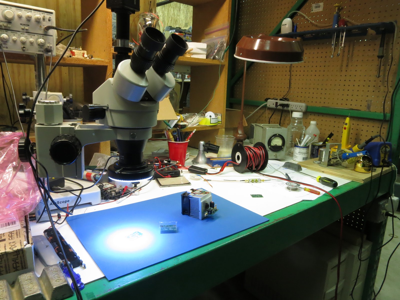
The Bench
Dishearted - I gave up - left the shop "without" putting away my tools and cleaning up (I normally always clean up before leaving).

Bummer!!

Several days have past (about a week), it is now Sunday and I am planing to go to Jack's Homebrew Club evening meeting on Tuesday, and the following night I am going to the pQRP monthly meeting. I decided to clean-up the PA (to remove excess solder flux) to make it "look good", and take it to the two meetings, to show my epic FAILURE of a nice idea for the PA.

While cleaning the circuit board, I noticed one of the legs of the (necessarily) "dead bug" mounted transistors did NOT appear to be soldered (with filets) to its pad, it appeared to have just a glob (flyspeck) of solder on the bent leg. This was the drive transistor for the output power FET, maybe it was not actually soldered down!!

For me, it is actually quite difficult to see a single SOT-23 pad without a Microscope.

Under the Microscope I could see it only had flux between the pin and pad!! I heated the soldering iron, fixed the joint, re-connected the Propeller Beacon Exciter, the output Low Pass Filter, the 50 Ohm Dummy Load, and the 12.6 Volt supply, . . .

WOW!, I observed 43 Volts PP at the load. That is; (43/2*.707)^2/50 = 4.7WATTS - YES!!!!!

Which is a gain of 25.93dB.

The PA-47 Curcuit with a Sziklai Pair Driver works!!

I installed the rest of the TR circuit and Relay on the under side of the PCB, but - DANG! The relay would not work! Now what??

After several hours, I discovered that I had attached the Relay Coil to the opposite pins on the Library PCB pads within DipTrace, the Relay is polarity sensitive. Like the drive transistors I had jury-rig the Relay by cross wiring the coil under it to make it work (the fix can not be see in the photo).

After cross-wiring the coil pins and re-installing the Relay - All worked as expected :-)
PA-47 - With TR Circuit and Relay Installed
Regardless of Success or my Failures, Tess is always watching, to make sure everything is being done right! She was not involved with the PA design or PCB layout, but some how she must have missed the poor solder joint!! (actually, . . . she is watching her ball that I placed on the bench :-). If I had her concentration (and other admiral attributes), I may have NOT missed the above critical project details :-))))

Tess - Doing Her Job,
Production, Test, and Final Inspection
I am , . . . ah, . . we are NOW both Happy Campers!

. . . . . Tess has her Ball, and I have my PA!

I will later post more PA-47 Project details. More testing, and more work is needed to install angle brackets to support the PCB.


UPDATE:

Increasing the DC supply of up to 14.2 Volts (via a heavy duty Lead Acid Battery on a Charger), I got 60 Volts PP at the 50 Ohm Load, (60/2*.707)^2/50 = 9.0 WATTS- Nice!!

Note to self:
A Fan control via the TR circuit or HeatSink Temp would be useful, it would save some power and would be quieter.

UPDATE:

Here is the PA-47 running on Jack's Bench at his Homebrew Club meeting, the photo was taken by Jack and who suggested this photo would make a great (complex) puzzle picture :-)
PA-47 Running on Jack's Bench

--

Monday, November 26, 2012

PCB Solder Jumpers - Cont'd

For Diptrace my new (proposed) Solder Jumper (see previous post), the buried trace connection point on the pad was created by creating the "shape" with the "initial point" at the desired connection point. The "initial point" is where the construction of the "shape" starts and ends. After construction, the "shape" is converted to a "pad" via a right mouse menu item. Below, for demonstration, the "initial point" was artificially exposed by opening (moving) the adjacent points at the left. The grid is set to 2 mils.

For Demonstration the Trace
Connection Point is Exposed at the Cursor

Normally, the gap would be closed, and the two (moved) points would be located at the same point.

This use of the "initial point" may be documented some place in the Diptrace manuals, but I have not found it.

--

Saturday, November 24, 2012

PCB Solder Jumpers

I have received some good feedback on Patterns for PCB Solder Jumper (see previous posts).

Experiments with very small 0201 size foot prints were NOT as successful as I would like. The small 0201 pads would not hold enough solder to allow proper bridging of the gap between pads. A usable bridge could only be made with very dry slaggy solder.

I am trying the new Solder Jumper Pattern as I suggest in the previous post. Here are the proposed dimensions, the folded pads should help hold the solder and aid in bridge creation. Or, at least that is the plan.
Overall size is 72 x 32 mils (0703)
Dimension Values Shown are Mils
The trace connection is a point within the thicker section on each end. Finding the method of creating that point was via trial and error. Diptrace uses the first created pattern point as the attachment point, I had to artificially bury the point inside of the pad to make trace connections easy.

The PCB Manufactures that I use, and my own Homebrew PCB processing, should be able to create the pattern without difficulty.

I have recently sent a small board off to Manufacturing with one of these new Solder Jumpers ,  Soon, I will report the results.

--

Thursday, November 8, 2012

My Preferred Soldering Iron

Several years ago, my very old and faithful Weller finally died, and its replacement, the Wahl - Cordless also died (or was dying). I had always wanted a Hakko 888, so I put one on order along with several tips, of different types and sizes.

But I needed a reliable Soldering Iron for a project that I was working on, and I needed the Soldering Iron NOW! I could not wait for the postal service!

So, I went to Radio Shack or Frys (do not remember which) and found a Hakko 980-V12/P to finish my project. I thought it would be a good (junker) backup iron, as it uses the same tips as the Hakko 888 that I had on order (so I thought, . . . NOT). Well it does not! The tips are different.

Now, after many months of having all three Irons on the bench, I prefer the cheap Hakko 980 (with the standard tip) for most things that I solder, even down to the occasional 0201 resistors. Most of my projects use 0804 or 0603 parts. I use the same old stand that I used with the Weller, along with the wire pad tip cleaner. The new Hakko 888 is very seldom turned on.
Hakko 980 on the far Left
Hakko 888 on the Right

Wahl at the Upper Right
The Hakko 980 has dual heat modes; 20w and 130w. A simple push of a button increases the heat, and only if necessary (very seldom used). A one or two second press of the yellow button on the handle, is generally all that is ever needed.

My dying Wahl is standing in the back (yellow, upper right), it was nice for a while, but its finger switch became too temperamental and needs constant attention, see previous post.

Knowing what I know now, if I were buying a Soldering Iron - I would ONLY buy the Hakko 980-V12/P, which is much cheaper than a Hakko 888, and more reliable than the Wahl.


UPDATE

For reference, I originally provided Amazon links for the Hakko Soldering Irons listed on this post, but now it appears that all of my links are no longer working (what up with that, Amonzon?), so I replaced them with generic Google Links. I hope the Hakko 980 is actually still available?

--

Monday, November 5, 2012

Bypass Caps

The questions is; where to put Bypass caps in the circuit?

Next to a analog or digital device of course, between the VCC and VSS pins.

But, this is only really easy to do on; push boards, protoboards, deadbug or experimental circuits, just push the caps in, and/or solder as necessary.

But then, if you are actually planning to build a complex PCB's (i.e. more than a few devices), it is a lot of work to make sure the right cap (as per the schematic) is next to its associated device. All of the bypass caps are connected in parallel to the same supply and ground rails (i.e. VCC and VSS), therefore on the initial PCB layout they are connected to the same "rats nest" and not really associated with a particular device. The unscrambling task is even more difficult, because bypass caps are typically all the same value.

Some designers just scatter the bypass caps around the board next to a likely devices. Other (better) designers take the time to place the correct bypass caps near its associated devise, as per the schematic - this can be a lot of work!

But, does it matter? - it is only a reference symbol printed on PCB in silkscreen. To me; "Yes, it does matter". And therefore, I make sure the correct bypass cap is next to its associated device as per the schematic.
Schematic Diagram

I use the following technique to make the PCB layout of bypass caps and associated devices easy. On the schematic, I insert a "Zero Ohm" resistor in the supply line (VCC) that feeds each bypass cap. Now regardless of PCB layout software that is used, the initial "rats nest" will suggest close layout of the correct bypass cap with its associated device. From PCB layout perspective, the Bypass caps are NOT directly attached to the VCC rail, but instead, it is connected to the "Zero Ohm" resistor which is connected to the power VCC rail. The associated "Zero Ohm" series resistor is easily located and placed next to its bypass cap (because it is in series and not parallel on the schematic). Its a simple trick that just makes PCB layout much-much easier!

PCB Layout

Also, for most low current devices where 6 mil traces are typical, I use a 0201 "Zero Ohm" device footprint. Instead of an actual device, a simple solder bridge is all that is needed to make the connection. And, this technique makes troubleshooting a new designs all that much easier. A troubling device can be removed from the circuit with a little solder wick.
As Manufactured

As seen in the schematic diagram, B2 is the symbol that I created for the solder bridge.


This technique; may, or may not, be useful for Production Products, but for the Hobbyist it works great!

BTW, I also put in 0201 "Zero Ohm" in all I2C lines, next to each I2C device, for easy initial testing. A bad I2C device can easily take the entire bus down - which is not fun to troubleshoot.


UPDATE

Note: I am looking for a more appropriate footprint for an easy to use solder jumper.

A "Zero Ohm" resistor can also be used to enforce and make easier a "star grounding" system for a set of parts. Connect the circuits star grounds to one end of the "Zero Ohm" resistor and the real ground to the other. For a PCB layout, a star isolated ground plane can also be attached to the same point (i.e., multiple isolated ground planes can be used on the same board).

UPDATE 2

I am considering one of the following for future project Solder Jumpers, some additional function and use evaluation is needed.
Proposed Solder Jumpers
  • Jumper SJ2 is about 100 mil diameter with 10 mill isolation.
  • Jumper SJ1 is a 70x40 mil rectangle with 6 mil isolation.
-

Saturday, November 3, 2012

A Self Photo from Mars - at 41.5M Pixels

OK, this is another Curiosity photo, But,  it is an Absolutely Amazing High Resolution Self Photo taken on Mars.


This photo was stitch together from many smaller photos. The Detail is stunning at 5463 x 7595 pixels that is a 41.5M pixel image !!

Go to the link, it may take a while to download, but zoom in and pan around to see the high resolution details !

For Ham Radio QRP, Hardware, and Robotic Geeks - it does not get better than this !

Thanks JPL and NASA !!

Now we need someone to explain all of the devices on the Rover, like:

  • What is that waveguide driven vertical antenna on the back left-side of the rover (upper right in the photo)?
  • What are thosee funnel shaped cones on the front? Are those small linear actuators used for positioning?
  • What is that Large Grey Cross bar on the Top?

And, maybe someone will make a Trimble (Google) Sketchup of the Rover ?

-

More Fun with 3D

I recently updated a previous post showing the outside view from my loft. The original photo was taken on Sep 16th, and now the second was taken on Nov 2ed, These photos are arranged for Cross-Eye 3D viewing (CE3D). I took this last photo just because of the very bright fall colors. Not wanting to bore my blog readers with "just another one of my 3D photos", I decided to attach it to a previous blog page (nobody other than myself will really notice).

But, I inadvertently discovered a very interesting artifact of publishing them on the same post page; after clicking on the first image for the expanded browser view, you can quickly flip between the two views with a gentle roll of the middle mouse button. For this scene, only the season's colors change (and maybe a slight unintended zoom scale). The effect can be seen in 2D, but it is not nearly as dramatic as seen in 3D.

Even with only two photos, the time lapse photography is very intriguing in 3D. I now plan to take similar photos at regular intervals to expand the time frame. Maybe a new photo set each week.

I use ImageMagick to combine the Right and Left images into a CE3D view. For example:

convert R.JPG L.JPG -splice 10x0 +append -chop 10x0 -resize 1200  CE3D.JPG

Note: the Right/Left order of the two original images is very important.

Oh, I have been viewing so many Cross-Eye 3D Viewed photos that I now can quickly switch to Cross-Eye 3D mode and without Eye Strain. The images are photos that I have taken, or created from the raw Mars Mission photos, and others found on the web,  I view most online images from about 30 inches (distance to the computer screen).

I like 3D photos, they provide so much more revealing detail, that just can not be perceived in 2D. It is similar to the different listening pleasures of; an AM Mono broadcast, and good a FM Stereo Music Station.

I plan to do a lot more with this interesting viewing mode.

Here is an interesting Cross-Eye 3D Video that may help explain the viewing technique.

-

Sunday, October 28, 2012

I Abandoned Nvidia for My Ham Station Computers

I use Ubuntu on my Ham Shack Computers, and have recently installed the new revision 12.04. All of my Ham Applications seem to work much better with this new release, the sound system seems to work predictably and correctly.

But, I gave up on graphics, after several days of frustration trying to get my Nvidia G7000 Graphics Card to work in the 3D mode on Ubuntu (see previous post).

I decided to try to replace the "Nvidia Graphics Card" with my Son's discarded and dying "ATI Radeon HD 5450" graphics card. A little repair of the card's fan and a little micro surgery was necessary to bring the "ATI Radeon" roaring back to life.

I installed the repaired ATI Radeon card, rebooted and it worked as expected in 2D mode. I then installed the suggested Drivers, and rebooted, - it just worked!  -  No hassle nor pain, Ubuntu graphics now runs in the 3D mode!

After much research, I found that; due to lack of manufactures supported or open drivers, the Nvidia Cards are not well supported for use with Ubuntu. For my other system upgrades, I am going to abandon Nvidia in favor of ATI.

I really like the new 3D Graphics menus and workspaces!

Note: The menus do not actually appear in 3D, but Ubuntu does use the graphics card's 3D processor to quickly and dynamically display the menus and workspaces. In 2D mode, some functionality is not available.

--

Saturday, October 20, 2012

My Update to Ubuntu 12.04

Last weekend my Son, requested help installing Ubuntu on one of his old Laptops and an old Workstation. He has only used MS up until now. I have always used some flavor of Linux for most of my systems from the beginning  (as far back as Minux). For my Son, I suggested Ubuntu as that is what I have been using for the last few years, and it is easy to admin!

I have been using Ubuntu 10.04 LTS since 2010 (as implied by the Rev Number). The LTS suffix means that the Rev has what is called "Long Term Support" from developers. I like LTS as it is more likely to be stable. Because I am mostly satisfied with my Ubuntu installation, I had not kept up with the latest news of additional releases. But, for my Son new installations I wanted to review the latest available release. To my pleasant surprise the current Rev of Ubuntu is 12.04 with LTS.  I should have known as it is a even numbered release. For those that do not know, the first two digits of the Rev number is the year and the last is the month. The developers plan is an LTS for each even numbered year.

To me this is good news, I could install Ubuntu 12.04 on my Son's fresh wiped systems, before I would have to figure out how to do the same on my established systems.

We downloaded the ~700MByte Ubuntu 12.04.1 ISO file, to my Laptop and proceeded to transfer the file to a USB  thumb drive. But we could not get his older workstation to boot from the USB. The solution should be simple; transfer the image to CD, but that did not work, the image is larger than a CD. A DVD is necessary, but that is OK as my laptop contains a DVD burner. The image was transferred onto the DVD, but then that did not work as the Workstation and Laptop could not use the image written at high speed. With some research,  the recommended speed was below 4X. A new DVD was burned at low speed. The Laptop install process was a little slow, but going well enough that a second DVD was burned to use with the Workstation. The Workstation was much faster than the Laptop and finished first. We then had fun playing and admin'ing the two new systems.

That night when I got home (about 10pm) I decided that was easy and therefore I should update my (established) Laptop. It would not be a fresh install, but an update, preserving as all of the user data. At about 3:30am when I went to bed,  I had still not completed the task. The next morning all went well and now I have a Laptop running Ubuntu 12.04.1 LTS.

I tried to do the same with one of my Workstation, to make a long story short, I attempted to update the system twice and scratch installed it four additional times, my user data was on another disk and therefore a install was not a great lose. In general, the problem and answers were: Build from DVD and not try to use an USB, the NVIDIA video card that the Workstation contains is not supported very well. Ubuntu 12.04 uses what is called Unity for windowing, the menus and workspaces are best viewed in the 3D mode, NVIDA 3D is not currently supported by Ubuntu.

Self Image

But, after many hours, I have Ubuntu 12.04.1 on two system, and to my surprise the major thing that I have always complained about Ubuntu, appears to be FIXED. Before at rev 10.40, the "sound" system seemed to never worked right, now it seem to just work -Yeah!

I am going to like Ubuntu 12.04.1 :-)

More details and progress may follow.

--

Friday, October 12, 2012

Litter Photographed on Mars

Sixty five days after landing, "Litter" was photographed on Mars.

The Litter appears to be a plastic tape fragment. Curosity's arm hand camera took the following close-up photo.

Litter found on Mars
The JPL crew is trying to determine the litter's origin. They are assuming it fell off of Curosity, and wondering "how or if " system integrity has been compromise. Read the full story here or see a video (mov) here.

It would be interesting to know if it was dropped here by Curosity, or debris scattered here as part of the Landing 65 days ago.

My questions are:
  • Did they bring a Trash Sack to collect their own Litter?
  • Do they plan to attempt retrieving the Litter?
  • How long do they think plastic will last on Mars?
Remember on Earth, the rule is:
Pack it in - Pack it out!

Ham Radio

I will get back to "Ham Radio Blogging" soon, I have several projects in the works, two PCB's being manufactured, and currently having fun attempting to gennerating PSK31 with the Prop.

--

Monday, September 17, 2012

Curiosity's First Major Rock Photos

On Sol0038 Curiosity took the first photo of a major rock along its path. Although, it may be just a layer of hard crusted dirt.
Curiosity's First Major Rock
From this and previous photos, it appears the Curiosity has been climbing up a very slight slope, with a some distance to go to the crest.

On Sol0040 it appears that Curiosity has almost made it to the the crest of the rise and then it will be going down hill for a while.
Near the Crest of the Rise
On the way to Mount Sharp
The slope of the land is not real apparent in the individual 2D images, only in 3D is it obvious.

Disclaimer: Raw Curiosity photos are available from the NASA web site,  Cross-Eyed Images above were constructed by Eldon Brown, with Image-Magick.

--

Sunday, September 16, 2012

More Local 3D Views

I have been playing some more with Cross-Eye 3D photos. This time the subject is the view out of my loft window. The lighting is not very good, but there are two Deer in the frame. They are very small and seen; below, and slightly to the right of the closest branch of the foreground tree. One is forward a little and laying down, the other is standing a little further back, looking over her left shoulder.
Deer Seen From My Loft
Sep 16, 2012
If I had known the deer were in the shot, I would have tried to use some zoom.

I found a easy way to take the two photos, slide the camera along a small angle of wood or something that is stable. My camera sits nicely and square against a supporting back lip. Between the two shots, I slid the camera about 3 or 4 inches.

Note: if you do not look at this in 3D, you may not determine the branch that I refereed to and therefore may not be able to see the Deer.

Here is an interesting Cross-Eye 3D Video that may help explain the viewing technique.


UPDATE:

Fall is in the air:
Nov 2, 2012
Nov 8, 2012
Nov 15, 2012
Nov 25, 2012 13:15
Dec 18, 2012 10:00
First Snow


--