My Son and I are working on a project that will use a microcontroller and air valves to control air cylinders. For the prototype, we need an output from the micro at 3.3 volt to drive the air selenoid at 12 volts. The circuit chosen consists of two transistors and a FET.
I created the small circuit using the Toner Transfer Method (TT) as shown below. For the prototype we only need one copy, but I always print more than necessary. Later twenty circuits will be ganged into a single circuit with single I2C input and an I/O expander to address each air valve.
 |
| Toner Transfer Method - Toner Still Attached each Circuit is 0.7 x 0.7 Inches |
But, I get very-very good results. Most of my Ham Radio TT PCB use 6 mil traces with 6 mil spacing, and with cross-hatched copper pour areas. I occasionally use solid copper pour with equally good results. Note: this board uses larger traces.
 |
| Close Inspection - No Flaws |
Note: Double sided boards take only about twice as long to finish.
The only real concerns of DIY Toner Transfer Method created boards is; the lack of easy "Via" and plated holes. With a little creative design, most of these concerns can be worked-around, using part leads and short wire though some holes.
I find Toner Transfer Method boards; Quick, Easy, Fun, Satisfying and with good Quality - I recommend TT for all hobbyist.
I am considering creating a video of my process, showing that very good results can actually be achieved.
UPDATE: Feb 1, 2014
Actually, the circuit works much better than expected :-)
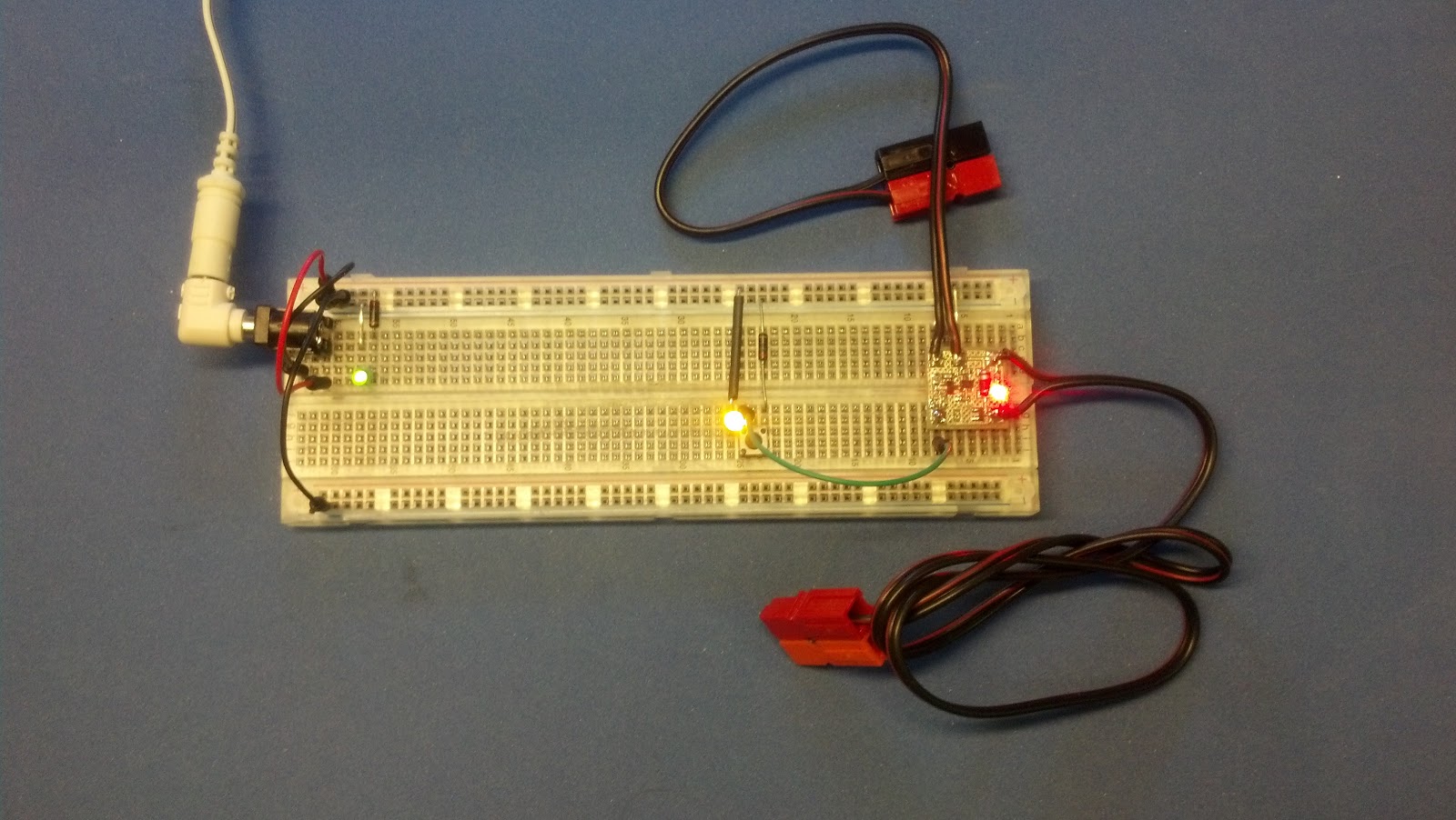 |
| The Circuit is still on the Test Fixture Normally, Power is applied to the top Power Pole Connector and a Solenoid will be attached to the lower Power Pole |
 |
| LED Indicates that the Output is ON |
--
Nice project. I have some Kinsten brand pre-sensitised PCBs I'm going to use for some RF projects (between 100 and 200 MHz) but I'm not sure exactly how I should select my trace dimensions.
ReplyDeleteI was wondering how you decided on 6 mil traces with a hatched (6 mil lines?) fill? Did you calculate with a specific dielectric constant for your boards, did you use a standard fibre-glass value, or did you simply use a hobbyist standard?